
New is the updated ddr4 memmory modules.
Also new is the new and old for apple computers the so called thunderbold connection.
Wich is faster then usb3.1.
As seen on asus rog motherboard series wich have the latest hardware use.
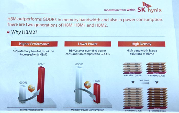
Also new is the already excisted amd ati,s hbm 2 memmory modules who are present still so far only on amd ati videocards.
And ofcorse we have the k multiple core technologies processors from intel who fit this new hardware as a glove.
asus rog motherboard series
https://www.asus.com/nl/Motherboards/MA ... I_FORMULA/
hbm 2 memmory
https://en.wikipedia.org/wiki/High_Band ... mory#HBM_2
hbm 2 text version:
Spoiler
HBM 2[edit]
On January 12, 2016 HBM 2 was accepted as JESD235a.[7]
HBM 2 specifies up to 8 dies per staple and doubles throughput to 1 TB/s.
On January 19th, 2016, Samsung announced early mass production of HBM2.[8][9] HBM2 is predicted to be especially useful for performance sensitive consumer applications such as virtual reality.[10]
History[edit]
AMD Fiji, the first GPU to use HBM.
The development of High Bandwidth Memory began at AMD in 2008 to solve the problem of ever increasing power usage and form factor of computer memory. Amongst other things AMD developed procedures to solve the die stacking problems with a team led by Senior AMD Fellow Bryan Black. Partners from the memory industry (SK Hynix), interposer industry (UMC) and packaging industry (Amkor Technology and ASE) were obtained to help AMD realize their vision of HBM.[11] High volume manufacturing began at a Hynix facility in Icheon, Korea in 2015.
HBM has been adopted as industry standard JESD235 by JEDEC as of October 2013 following a proposal by AMD and SK Hynix in 2010.[4] The first chip utilizing HBM is AMD Fiji which was released on June 24, 2015 powering the AMD Radeon R9 Fury X.[12]
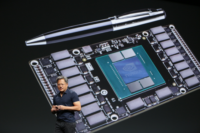
The world's first GPU chip utilizing HBM2 is Nvidia Tesla P100 which was officially announced on April 5, 2016.[13]
On January 12, 2016 HBM 2 was accepted as JESD235a.[7]
HBM 2 specifies up to 8 dies per staple and doubles throughput to 1 TB/s.
On January 19th, 2016, Samsung announced early mass production of HBM2.[8][9] HBM2 is predicted to be especially useful for performance sensitive consumer applications such as virtual reality.[10]
History[edit]
AMD Fiji, the first GPU to use HBM.
The development of High Bandwidth Memory began at AMD in 2008 to solve the problem of ever increasing power usage and form factor of computer memory. Amongst other things AMD developed procedures to solve the die stacking problems with a team led by Senior AMD Fellow Bryan Black. Partners from the memory industry (SK Hynix), interposer industry (UMC) and packaging industry (Amkor Technology and ASE) were obtained to help AMD realize their vision of HBM.[11] High volume manufacturing began at a Hynix facility in Icheon, Korea in 2015.
HBM has been adopted as industry standard JESD235 by JEDEC as of October 2013 following a proposal by AMD and SK Hynix in 2010.[4] The first chip utilizing HBM is AMD Fiji which was released on June 24, 2015 powering the AMD Radeon R9 Fury X.[12]
The world's first GPU chip utilizing HBM2 is Nvidia Tesla P100 which was officially announced on April 5, 2016.[13]
The new hbm 2 memmory usages will be only avaleble for the highend marked.
The new amd ati videocard is avaleble for 1700,00 euro and is realy now at the top segment.
When nvidia comes out wich socha memmory avaleble for nvidia videocards for the gaming marked is unknow.(maby they making it right now)
as in for the older technologie combines with the ddr5 and ddr5x memmory modules wich are mass produced right now.
If you WANT that hbm 2 memmory modules on your new videocard you can bether waith.
Becous we all know that what comes comes out early then you will pay for it.
Spoiler
http://hexus.net/media/uploaded/2015/7/ ... d607aa.jpg
hbm1 and hbm2 memmory usage:
Spoiler

http://www.extremetech.com/gaming/21822 ... -bandwidth
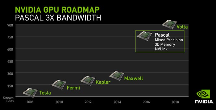
pascal gp 100
Spoiler
While Nvidia is not opening up about the details, and Pascal GP100 is going to take more than a few months to be out in thee open, predictions are what we will be relying on for the Nvidia Pascal GPU specifications.
VideoCardz has done the hard work for us on this. Assuming a couple of things like what could be the architecture’s positioning, that the whole thing is based on a similar solution to Maxwell and Kepler in terms of GPC splitting.
So firstly, they are suggesting that in comparison to three Streaming Multiprocessors per Graphics Processing Cluster of Kepler and four that of Maxwell, the Pascal GPU specifications include six Streaming Multiprocessors per Graphics Processing Cluster.
However, Kepler has 192 CUDA/SM and Maxwell has 128 which compares to a very low 64 CUDA/SM of Pascal. CUDA/GPC also varies proportionately at 576 and 512 for the existing architectures and 384 for Pascal.
For Pascal GP100, in terms of enthusiast Nvidia GPUs, the Die Size is 610 mm2 with 15.3 billion transistors resulting in 25.08 million transistors/mm2.
They also talk of Pascal GP104 where the die size is approximately between 350-400 mm2 (most probably around 400) and approximately 10.2 billion transistors with 4 GPCs, 40 SMs and 2560 CUDAs.
Moving on to Mid-range Pascal GP106; it is expected to have a die size between 190 to 215, with approximately 5.4 billion transistors, 2 GPCs, 20 SMs and 1280 CUDAs. Suggesting a smaller bump over GM206.
Lastly, we have the entry level Pascal GP107 where a 120-150 mm2 die size is predicted with 3.5 billion transistors, 1 GPC, 10 SMs and 640 CUDAs.
While that is all we have for Nvidia Pascal GPU specifications predictions right now, we will be more informed in the coming days and weeks.
But you are very sure you can have this computer for the last 5 years without buying a new 1.
i,m sure there are motherboards wich have the same specs as asus rog if so not they are under devolpment.
happy reading and be amased about this hardware.
edit typo forgotten


